- 您现在的位置:买卖IC网 > Sheet目录3874 > PIC16LF724-E/PT (Microchip Technology)IC PIC MCU FLASH 7KB 44-TQFP
2009 Microchip Technology Inc.
DS41341E-page 113
PIC16F72X/PIC16LF72X
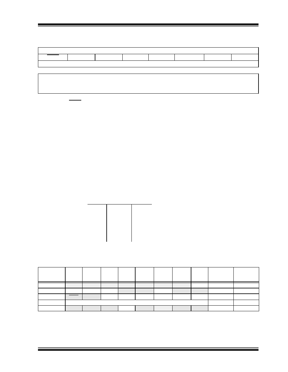
TABLE 11-1:
SUMMARY OF REGISTERS ASSOCIATED WITH TIMER0
REGISTER 11-1:
OPTION_REG: OPTION REGISTER
R/W-1
RBPU
INTEDG
T0CS
T0SE
PSA
PS2
PS1
PS0
bit 7
bit 0
Legend:
R = Readable bit
W = Writable bit
U = Unimplemented bit, read as ‘0’
-n = Value at POR
‘1’ = Bit is set
‘0’ = Bit is cleared
x = Bit is unknown
bit 7
RBPU: PORTB Pull-up Enable bit
1
= PORTB pull-ups are disabled
0
= PORTB pull-ups are enabled by individual port latch values
bit 6
INTEDG: Interrupt Edge Select bit
1
= Interrupt on rising edge of INT pin
0
= Interrupt on falling edge of INT pin
bit 5
T0CS: TMR0 Clock Source Select bit
1
= Transition on T0CKI pin or CPSOSC signal
0
= Internal instruction cycle clock (FOSC/4)
bit 4
T0SE: TMR0 Source Edge Select bit
1
= Increment on high-to-low transition on T0CKI pin
0
= Increment on low-to-high transition on T0CKI pin
bit 3
PSA: Prescaler Assignment bit
1
= Prescaler is assigned to the WDT
0
= Prescaler is assigned to the Timer0 module
bit 2-0
PS<2:0>: Prescaler Rate Select bits
000
001
010
011
100
101
110
111
1 : 2
1 : 4
1 : 8
1 : 16
1 : 32
1 : 64
1 : 128
1 : 256
1 : 1
1 : 2
1 : 4
1 : 8
1 : 16
1 : 32
1 : 64
1 : 128
BIT VALUE
TMR0 RATE
WDT RATE
Name
Bit 7
Bit 6
Bit 5
Bit 4
Bit 3
Bit 2
Bit 1
Bit 0
Value on
POR, BOR
Value on
all other
Resets
CPSCON0
CPSON
—
CPSRNG1 CPSRNG0
CPSOUT
T0XCS
0--- 0000
INTCON
GIE
PEIE
T0IE
INTE
RBIE
T0IF
INTF
RBIF
0000 000x
OPTION_REG
RBPU
INTEDG
T0CS
T0SE
PSA
PS2
PS1
PS0
1111 1111
TMR0
Timer0 Module Register
xxxx xxxx
uuuu uuuu
TRISA
TRISA7
TRISA6
TRISA5
TRISA4
TRISA3
TRISA2
TRISA1
TRISA0
1111 1111
Legend:
– = Unimplemented locations, read as ‘0’, u = unchanged, x = unknown. Shaded cells are not used by the Timer0 module.
发布紧急采购,3分钟左右您将得到回复。
相关PDF资料
PIC18LF44J10T-I/ML
IC PIC MCU FLASH 8KX16 44QFN
PIC16LF727-I/PT
IC PIC MCU FLASH 8K 1.8V 44-TQFP
PIC24F08KA102-I/SO
IC PIC MCU FLASH 8K 28-SOIC
PIC18LF44J10T-I/PT
IC PIC MCU FLASH 8KX16 44TQFP
PIC24F16KL401-I/SO
IC MCU 16BIT 16KB FLASH 20-SOIC
PIC18LF25J10T-I/SS
IC PIC MCU FLASH 16KX16 28-SSOP
PIC16LF1527-I/PT
MCU PIC 28KB FLASH 64TQFP
PIC18F25K20-I/SP
IC PIC MCU FLASH 16KX16 28-DIP
相关代理商/技术参数
PIC16LF724-I/ML
功能描述:8位微控制器 -MCU 7KB Flash Prog 16MHz Int Osc 1.8V-5.5V
RoHS:否 制造商:Silicon Labs 核心:8051 处理器系列:C8051F39x 数据总线宽度:8 bit 最大时钟频率:50 MHz 程序存储器大小:16 KB 数据 RAM 大小:1 KB 片上 ADC:Yes 工作电源电压:1.8 V to 3.6 V 工作温度范围:- 40 C to + 105 C 封装 / 箱体:QFN-20 安装风格:SMD/SMT
PIC16LF724-I/MV
功能描述:8位微控制器 -MCU 7KB Flash RAM 192b nanoWatt RoHS:否 制造商:Silicon Labs 核心:8051 处理器系列:C8051F39x 数据总线宽度:8 bit 最大时钟频率:50 MHz 程序存储器大小:16 KB 数据 RAM 大小:1 KB 片上 ADC:Yes 工作电源电压:1.8 V to 3.6 V 工作温度范围:- 40 C to + 105 C 封装 / 箱体:QFN-20 安装风格:SMD/SMT
PIC16LF724-I/P
功能描述:8位微控制器 -MCU 7KB 1.8-3.6V 16MHz 8b ADC CCP Lo Pwr
RoHS:否 制造商:Silicon Labs 核心:8051 处理器系列:C8051F39x 数据总线宽度:8 bit 最大时钟频率:50 MHz 程序存储器大小:16 KB 数据 RAM 大小:1 KB 片上 ADC:Yes 工作电源电压:1.8 V to 3.6 V 工作温度范围:- 40 C to + 105 C 封装 / 箱体:QFN-20 安装风格:SMD/SMT
PIC16LF724-I/PT
功能描述:8位微控制器 -MCU 7KB 1.8-3.6V 16MHz 8b ADC CCP Lo Pwr
RoHS:否 制造商:Silicon Labs 核心:8051 处理器系列:C8051F39x 数据总线宽度:8 bit 最大时钟频率:50 MHz 程序存储器大小:16 KB 数据 RAM 大小:1 KB 片上 ADC:Yes 工作电源电压:1.8 V to 3.6 V 工作温度范围:- 40 C to + 105 C 封装 / 箱体:QFN-20 安装风格:SMD/SMT
PIC16LF724T-I/ML
功能描述:8位微控制器 -MCU 7KB Flash Prog 16MHz Int Osc 1.8V-5.5V
RoHS:否 制造商:Silicon Labs 核心:8051 处理器系列:C8051F39x 数据总线宽度:8 bit 最大时钟频率:50 MHz 程序存储器大小:16 KB 数据 RAM 大小:1 KB 片上 ADC:Yes 工作电源电压:1.8 V to 3.6 V 工作温度范围:- 40 C to + 105 C 封装 / 箱体:QFN-20 安装风格:SMD/SMT
PIC16LF724T-I/MV
功能描述:8位微控制器 -MCU 7KB Flash RAM 192b nanoWatt RoHS:否 制造商:Silicon Labs 核心:8051 处理器系列:C8051F39x 数据总线宽度:8 bit 最大时钟频率:50 MHz 程序存储器大小:16 KB 数据 RAM 大小:1 KB 片上 ADC:Yes 工作电源电压:1.8 V to 3.6 V 工作温度范围:- 40 C to + 105 C 封装 / 箱体:QFN-20 安装风格:SMD/SMT
PIC16LF724T-I/PT
功能描述:8位微控制器 -MCU 7KB Flash Prog 16MHz Int Osc 1.8V-5.5V
RoHS:否 制造商:Silicon Labs 核心:8051 处理器系列:C8051F39x 数据总线宽度:8 bit 最大时钟频率:50 MHz 程序存储器大小:16 KB 数据 RAM 大小:1 KB 片上 ADC:Yes 工作电源电压:1.8 V to 3.6 V 工作温度范围:- 40 C to + 105 C 封装 / 箱体:QFN-20 安装风格:SMD/SMT
PIC16LF726-E/ML
功能描述:8位微控制器 -MCU 14KBFlash Prog 16MHz Int Osc 1.8V-5.5V
RoHS:否 制造商:Silicon Labs 核心:8051 处理器系列:C8051F39x 数据总线宽度:8 bit 最大时钟频率:50 MHz 程序存储器大小:16 KB 数据 RAM 大小:1 KB 片上 ADC:Yes 工作电源电压:1.8 V to 3.6 V 工作温度范围:- 40 C to + 105 C 封装 / 箱体:QFN-20 安装风格:SMD/SMT